Contact : Géraldine HALLAIS, in collaboration with HETERNA Team : Charles Renard, Laetitia Vincent & Daniel Bouchier
This epitaxy growth equipment is mainly used for the development of nano and micrometric hetero-structures based on semiconductor elements of columns III-IV-V integrated on silicon substrate for photovoltaic, thermoelectric, microelectronic and photonic applications.
It is compatible with Si substrates of 4 and 8 inches.
It includes:
- An introductory airlock surrounded by a nitrogen glove box
- A chamber UHV for chemical deposition in vapour phase (UHV-CVD) with RHEED in-situ (Reflection High Energy Electron Diffraction) device
- A chamber UHV for chemical beam epitaxy (CBE) with RHEED in-situ
- One XPS/AES (X-Rays Photolélectrons Spectrometry, Auger Electrons Spectrometry) surface characterization chamber
Hydrides (silane, germane, digermane...) or organometallics (tributylarsine, trimethyl gallium, trimethylAluminium, triethylgallium and trimethylindium...) are involved in the two CVD and CBE deposition techniques, which will decompose on the surface of the hot substrate on which growth is desired. The molecules on the surface will break down into subspecies. Hydrogen or Cxhy radicals will evaporate and be evacuated by the pumping system. The III-IV or V elements of the precursor molecule go in turn, and if the deposition conditions are well chosen (temperature and pressure) integrate into the crystal.
The advantages of these techniques are: a good quality of the film deposited, a good homogeneity and reproducibility, a high deposition speed.
The RHEED devices allow to check the state of deoxidation of the substrate after annealing, or to check during growth the crystalline state of the deposited layers.
A fourth ultravacuum chamber of the equipment has a SEM column and an XPS system with an X-ray source (Twin anode Mg and Al) and a hemispherical spectrometer. The XPS allows to obtain the chemical composition of a surface of a material (< 10nm) by exciting it by RX and recovering the spectrum of the emitted photoelectrons. The nature of the chemical bonds and the atomic percentages are obtained by a significant treatment of the spectra obtained.
To obtain more localized surface chemical information, Auger spectrometry has been developed: in this case the sample is excited by the electrons of the SEM column and the Augers electrons are recovered by the XPS detector. Auger SAM (Scanning Auger Microscopy) imaging can be performed at µm resolution.

This equipment has a great versatility, and is equipped with in-situ XPS, Auger, and AES analyzes systems. We use it for different kinds of material studies :
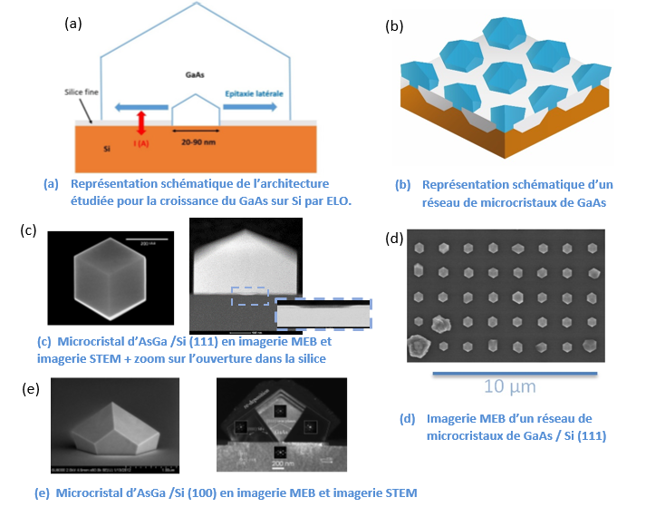
ELO consists in starting growth from a reduced opening in a very fine silica, the disagreed crystal is free to accommodate its lattice parameter. So only the germ is nanometer, the final crystal can be microscopic in size.
Example: Integration of AsGa crystals by ELO through nano openings in a very thin layer of Sio2 (0.6 to 5nm).
Application: Study, Design and Optimization of a tandem GaAs/Si photovoltai(Projet ANR MULTISOLSI 2012-2017)
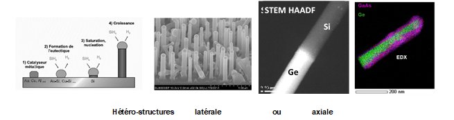
The nanowires in our equipement are obtained by the vapour-liquide method (LDS) with metallic drops as catalysts.
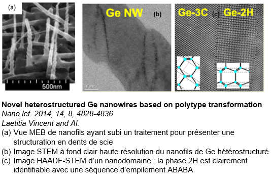
An example of applications: is Idex Nanoharvesting (2014-2016) and ANR HESXIGE (2017-2021) projects wich consist essentially to study the properties of heterostructured cubic/haxagonal nanowires (3C/2H) of Ge and Si.
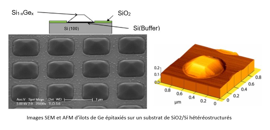
Example: selective epitaxy of pyramids SiGe with a Ge composition > at 20% in a hole size 1µmX1µm in a thin silica.
Application: detector of position (project with IRFU-CEA Saclay)
GeePs, CEMES, IRFU (CEA), INL, LPS, LOMA, SOLEIL, LPCIM
